Multilayer PCB Circuit Board With SMT &
DIP AssemblyOur Service1. PCB design ,PCB clone and copy
,ODM service.2. Schematic design and Layout3. Fast
PCB&PCBA prototype and Mass Production4. Electronic
Components Sourcing Services5. PCB Assembly
Services:SMT,DIP&THT,BGA repair and reballing6. ICT,
Constant Temperature Burn-in and Function Test7.
Stencil,Cables and Enclosure building8.
Standard Packing and On time Delivery PCB (PCB
Assembly) process capabilityTechnical RequirementProfessional
Surface-mounting and Through-hole soldering TechnologyVarious sizes
like 1206,0805,0603 components SMT technologyICT(In Circuit
Test),FCT(Functional Circuit Test) technologyPCB Assembly With
UL,CE,FCC,Rohs ApprovalNitrogen gas reflow soldering technology for
SMTHigh Standard SMT&Solder Assembly LineHigh density
interconnected board placement technology
capacityQuote&Production RequirementGerber File or PCB File for
Bare PCB Board FabricationBom(Bill of Material) for
Assembly,PNP(Pick and Place file) and Components Position also
needed in assemblyTo reduce the quote time, please
provide us the full part number for each
components,Quantity per board also the quantity for orders.Testing
Guide&Function Testing method to ensure the quality to reach
nearly 0% scrap rateOEM/ODM/EMS ServicesPCBA, PCB assembly: SMT &
PTH & BGAPCBA and enclosure designComponents sourcing and
purchasingQuick prototypingPlastic injection moldingMetal sheet
stampingFinal assemblyTest: AOI, In-Circuit Test (ICT), Functional
Test (FCT)Custom clearance for material importing and product
exportingOther PCB Assembly EquipmentsSMT Machine: SIEMENS
SIPLACE D1/D2 / SIEMENS SIPLACE S20/F4Reflow Oven: FolunGwin
FL-RX860Wave Soldering Machine: FolunGwin ADS300Automated Optical
Inspection (AOI): Aleader ALD-H-350B,X-RAY Testing ServiceFully
Automatic SMT Stencil Printer: FolunGwin Win-5One-stop
SolutionFactory showFAQQ1: How do you make sure the quality of
the PCBs?A1: Our PCBs are all 100% test including Flying Probe
Test, E-test or AOI. Q2: What is the lead
time?A2: Sample needs 2-4 working days, mass production needs
7-10 working days. It depends on the files and
quantity. Q3: Can I get the best price?A3: Yes. To
help customers control cost is what we are always trying to
do. Our engineers will provide the best design to save PCB
material.Q4: What files should we provide
for a customized order?A4: If only need PCBs,
the Gerber files are needed; If need PCBA, both Gerber files and
BOM are needed;If need PCB design,all requirement details are
needed.Q5:Can I get a free sample? A5: Yes, Welcome to
experience our service and quality.You need make the payment at
first, and we will return the sample cost when your next bulk
order.Any other questions please contact us directly./* January 22,
2024 19:08:37 */!function(){function s(e,r){var
a,o={};try{e&&e.split(",").forEach(function(e,t){e&&(a=e.match(/(.*?):(.*)$/))&&1
Quality Multilayer PCB Circuit Board with SMT & DIP Assembly products, provide good price Multilayer PCB Circuit Board with SMT & DIP Assembly from .
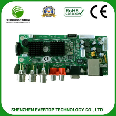
Larger photo of Multilayer PCB Circuit Board with SMT & DIP Assembly
Related products about Multilayer PCB Circuit Board with SMT & DIP Assembly
-
 Waste Tyre Plastic Recycling Machinery Machine Tire Crusher Production Line Rubber Crumb Grinding Machine Equipment Tire Shredder
-
 Stretch Plastic Blowing Pet Bottle Making Blow Molding Machine Bottles Stretch Automatic Pet Bottle Blowing Machine
-
 Waste Plastic Pet Bottle, Water Bottle Flake, PP/HDPE/LDPE PE Film Jumbo Woven Bags Plastic Crusher Machine, Plastic Crushing Washing Recycling Machine
-
 Type 2 Wall-Mounted Electric Car Charging Station 7kw /11 Kwelectric Vehicle Charging Station Home Wallbox AC EV Charger Single Phase or 3three Phase
-
 G-View G12W Wholesale Auto Car LED Headlight Bulb High Power H13 H11 9005 H7 H4 Car LED Headlights LED Car Lights
-
 New Design Porcelain Round Plates Dinner Set for Wedding and Banquet
-
 China 2023 New Design Super Soft 100% Polyester Microfiber Knitted Oversized Decoration Hoodie Blanket
-
 Handmade Art Creative Materials Thickened White Paper Cup DIY Disposable Handmade Colored Paper Cup


