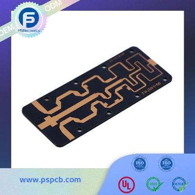
PCB ParametersItemPCB ParametersMaterialFR4 (140Tg, 170Tg,
180Tg), FR-406, FR-408, 370HR, IT180A, Metal Core, Polyimide,
Rogers 4350B/3003/4003C/5880, Taconic, Teflon, etcMaterial
BrandsKB, ITEQ, SY, ISOLA, Rogers (Arlon), Ventec, Laird, Nelco,
Bergquist, DENKA, Panasonic, Taconic, or other laminate on
customer's requestLayer Count1-40FlammailityUL 94V-0Thermal
Conductivity0.3W-300W/mkQuality StandardsIPC Classes 2/3HDI
Build-upAny Layer, up to 3+N+3Board Thickness0.2~7mmMin
Thickness2-layer: 0.2mm4-layer: 0.4mm6-layer: 0.6mm8-layer:
0.8mm10-layer: 1mmMore than 10 layers: 0.5*Layer Count*0.2mmCopper
Thickness0.5-20ozInksSuper White Inks/Solar/Carbon InksSolder Mask
Thickness0.2mil-1.6milSurface FinishesBare Copper, Hasl lead-free,
ENIG, ENEPIG, Gold Fingers, OSP, IAg, ISn, etcPlating
ThicknessHASL:Copper Thickness: 20-35um Tin: 5-20 umImmersion
Gold:Nickel: 100u"-200u" Gold: 2u" -4u"Hard Plated Gold:Nickel:
100u"-200u" Gold: 4u"-8u"Golden Finger:Nickel: 100u"-200u" Gold:
5u"-15u"Immersion Silver: 6u"-12u"OSP: Film 8u"-20u"Min Hole
Size0.15mmMin Trace Width/Spacing2mil/2milVia Plugging0.2~0.8mmLine
Width/Space Tolerance±10%Board Thickness Tolerance±5%Hole Diameter
Tolerance±0.05mmHole Location Tolerance±2milLayer to Layer
Registration2milS/M Registration1milAspect Ratio10:01Blind Vias
Aspect Ratio1:01Outline Tolerance±0.1mmV- CUT Tolerance±10miBevel
Edge± 5milWarp and Twist≤0.50% (max cap)Quality TestAOI, 100%
E-testValue-Added ServicesDFM Check, Expedited
ProductionFeatured ProcessesBonding, Impedance Control, Via in Pad,
Press Fit Hole, Countersink/Counterbore Hole, Castellated Vias,
Edge Plating, Peelable Solder Mask, Resin Plugged, Plating FlatData
FormatsGerber, DXF, PCBdoc, ODB++, HPGL, BRD, etc PCBA
AbilitiesItemPCBA AbilitiesTurnkey Service PCB Design + PCB
FAB + Components Sourcing + PCB Assembly + Package Value-Added
ServicesBOM Analysis, Conformal Coating, IC Programming, Wire
Harness & Cable Assembly, Box Building Assembly Details 5
SMT + 2 DIP (Dust and anti-static lines) Assembly AbilitiesSMT
5 million points per dayDIP 10 thousands pieces per
day Technical Support Free DFM/A check, BOM
analysis Handing Standards IPC-A-600H, IPC-A-610F,
J-STD-001FMOQ 1 piece Inspection & Testing Visual
Inspection, AOI, SPI, X-ray inspection. First article inspection
for each process. IQC + IPQC + FQC + OQC Inspection
Flow Flying probe test/In-circuit test/Function test/Burn-in
test Files We Need PCB: Gerber (CAM, PCB,
PCBDOC) Components: Bill of Material (BOM list) Assembly:
Pick-and-Place file Functional test: Test Guide PCB Panel
Size Min: 0.25×0.25 inches (6×6mm) Max: 20×20 inches
(500×500mm) PCB Solder Type Water soluble solder paste,
RoHS lead-freePCB Assemble MethodsSMT, THT & Hybrid, single or
double side placement, Part removal and
replacement. Components Details Passive down to 0201
(01005) size Press fit
connectors QFP/BGA/LGA/QFN/COB/COF CSP/WLCSP/POP Fine
Pitch High Pin Count Connectors BGA repair and
reball Lead Time Prototype: 5-15 working days; Mass
production: 20~25 working days. The fastest delivery time is 3
days. Packaging Anti-Static Bags/Customized
PackagingOne-Stop OEM PCB Assembly Professional Turnkey PCBA
COMPANY PROFILESPinsheng Electronics started to provide contract
electronics design and manufacturing services in 2008, we are
obsessed with providing the happiest manufacturing experience to
our customers.When our founders found it difficult to get technical
support and always high-quality products from the manufacturers,
they sprouted the vision to provide blissful electronics
manufacturing services to others, they rented an old workshop and
started the journey.In over 15 years, with the same vision, we have
designed, manufactured, and delivered 5,000+ projects for over
2,000 SMEs. The products are alive to us, not lifeless pieces of
stuff.Main CustomersMain Customers ProcessCasesUnderwater
Lighting·High thermal conductivity·Thermoelectric separation·0.15mm
Inner core·Micro bump etching·0.1mm Between FR4 and
copperIndustrial BMS·4-Layer PCB·6OZ Inner layer copper·Edge
plating·High current designEV Charger PileTurnkey PCB assembly for
control board of EV charger pile.Medical Equipment·Large area of
ENIG·Custom red soldermask·6-Layer rigid-flex boardCommunication
Equipment·6-Layer rigid-flex board·10% Differential
impedance·Ventec PPV447·ShengYi FR4·DuPont laminatedPCB
Showcase PCBA ShowcasePCBA ShowcaseSMT & DIP WorkshopSMT & DIP
WorkshopQuality And
Policy:Continually improve our quality, efficiency, service to satisfy thecustomer's requirement.Quality
System:1. ISO-9001:2018 Quality System Standard2. ISO14001
Environment System Standard3. Quality Standard: IPC-610-D class
2,4. Soldering Standard: J-STD-001 class 1,2,35. ESD Standard:
ESD-MIL-STD-16866. Workshop management:5S7. FAI-first article
inspection 8. In process visual inspection9. AOI inspection10.
X-ray Inspection11. SPI Inspection12. Machine calibration and
preventative maintenance13. ERP material and process managemen
Related products about PS Top Rank Printed Circuit Board PCBA Manufacturer High Frequency PCB Board
-
 Waste Tyre Plastic Recycling Machinery Machine Tire Crusher Production Line Rubber Crumb Grinding Machine Equipment Tire Shredder
-
 Stretch Plastic Blowing Pet Bottle Making Blow Molding Machine Bottles Stretch Automatic Pet Bottle Blowing Machine
-
 Waste Plastic Pet Bottle, Water Bottle Flake, PP/HDPE/LDPE PE Film Jumbo Woven Bags Plastic Crusher Machine, Plastic Crushing Washing Recycling Machine
-
 Type 2 Wall-Mounted Electric Car Charging Station 7kw /11 Kwelectric Vehicle Charging Station Home Wallbox AC EV Charger Single Phase or 3three Phase
-
 G-View G12W Wholesale Auto Car LED Headlight Bulb High Power H13 H11 9005 H7 H4 Car LED Headlights LED Car Lights
-
 New Design Porcelain Round Plates Dinner Set for Wedding and Banquet
-
 China 2023 New Design Super Soft 100% Polyester Microfiber Knitted Oversized Decoration Hoodie Blanket
-
 Handmade Art Creative Materials Thickened White Paper Cup DIY Disposable Handmade Colored Paper Cup


