PCBA Capabilities 1SMT assembly including BGA
assembly2Accepted SMD chips: 0204, BGA, QFP, QFN, TSOP3Component
height: 0.2-25mm4Min packing: 02045Min distance among BGA :
0.25-2.0mm6Min BGA size: 0.1-0.63mm7Min QFP space: 0.35mm8Min
assembly size: (X*Y): 50*30mm9Max assembly size: (X*Y):
350*550mm10Pick-placement precision: ±0.01mm11Placement capability:
0805, 0603, 040212High pin count press fit available13SMT capacity
per day: 80,000 points--Capability - SMT Lines 9(5
Yamaha,4KME)Capacity52 million placements per monthMax Board
Size 457*356mm.(18"X14")Min Component size 0201-54
sq.mm.(0.084 sq.inch),long connector,CSP,BGA,QFPSpeed 0.15
sec/chip,0.7 sec/QFP-Capability - PTH Lines2Max board
width400 mmType Dual wavePbs status Lead-free line
supportMax temp 399 degree CSpray flux
add-onPre-heat 3Production ProcessesMaterial
Receiving → IQC → Stock → Material to SMT → SMT Line Loading →
Solder Paste/Glue Printing → Chip Mount → Reflow → 100% Visual
Inspection → Automated Optical Inspection (AOI) → SMT QC Sampling →
SMT Stock → Material to PTH → PTH Line Loading → Plated Through
Hole → Wave Soldering → Touch Up → 100% Visual Inspection → PTH QC
Sampling → In-Circuit Test (ICT) → Final Assembly → Functional Test
(FCT) → Packing → OQC Sampling → ShippingOur AdvantagesHigh-end
equipment-high speed Pick and Place Machines that can process about
25,000 SMD components per hourHigh efficient supply ability 60K Sqm
monthly-Offers low volume and on-demand PCB production, also
large-scale productionProfessional engineering team-40 engineers
and their own tooling house, strong at OEM. Offers two
easy options: Custom and Standard-In-depth knowledge of IPC Class
II and III StandardsWe provide a comprehensive turn-key
EMS service to customers who want us to assemble the PCB into PCBA,
including prototypes, NPI projects, and small and medium volumes.
We are also able to source all components for your PCB assembly
project. Our engineers and sourcing team have rich experience in
the supply chain and EMS industry, with deep knowledge in SMT
assembly allowing us to resolve all the production issues. Our
service is cost-effective, flexible, and reliable. We have
satisfied customers across many industries including medical,
industrial, automotive, and consumer electronics.Quality
Control-Advanced equipment LISTAOI TestingChecks for solder
pasteChecks for components down to 0201Checks for missing
components, offset, incorrect parts, polarityX-Ray InspectionX-Ray
provides high-resolution inspection of:BGAs/Micro BGAs/Chip scale
packages /Bare boardsIn-Circuit TestingIn-Circuit Testing is
commonly used in conjunction with AOI minimizing functional defects
caused by component problems.Power-up TestAdvanced Function
TestFlash Device ProgrammingFunctional testing IOC incoming
inspectionSPI solder paste inspectionOnline AOI inspectionSMT's
first article inspectionExternal
assessmentX-RAY-welding inspectionBGA devise reworkQA
inspectionAnti-static warehousing and shipment-Persue 0% complaints
on the qualityAll department implements according to ISO and the
related dept has to provide an 8D report if any board is scrapped
to defective.All the outgoing boards have to be 100% electronic
tested, impedance tested, and soldering.Visually inspected, we make
the inspect microsection before shipment.Train the mindset of
employees and our enterprise culture, and make them happy with
their work and our company, it's helpful for them to produce good
quality products.High-quality raw material (Shengyi FR4, ITEQ,
Taiyo Solder Mask Ink, etc.)The AOI could inspect the whole set,
boards are inspected after each process PCB Technical &
Capability Production capacity of hot-sale productsDouble
Side/Multilayer PCB WorkshopAluminum PCB WorkshopTechnical
CapabilityTechnical CapabilityRaw materials: CEM-1, CEM-3,
FR-4(High TG), Rogers, TELFONRaw materials: Aluminum base, Copper
baseLayer: 1 layer to 32 LayersLayer: 1 layer and 2 LayersMin.line
width/space: 3mil/3mil(0.075mm/0.075mm)Min.line width/space:
4mil/4mil(0.1mm/0.1mm)Min.Hole size: 0.1mm(dirilling hole)Min. Hole
size: 12mil(0.3mm)Max. Board size: 1200mm* 600mmMax.Board size:
1200mm* 560mm(47in* 22in)Finished board thickness: 0.2mm-
6.0mmFinished board thickness: 0.3~ 5mmCopper foil thickness:
18um~280um(0.5oz~8oz)Copper foil thickness: 35um~210um(1oz~6oz)NPTH
Hole Tolerance: +/-0.075mm, PTH hole Tolerance: +/-0.05mmHole
position tolerance: +/-0.05mmOutline Tolerance: +/-0.13mmRouting
outline tolerance: +/ 0.15mm; punching outline tolerance:+/
0.1mmSurface finished: Lead-free HASL, immersion gold(ENIG),
immersion silver, OSP, gold plating, gold finger, Carbon
INK.Surface finished: Lead free HASL, immersion gold(ENIG),
immersion silver, OSP etcImpedance control tolerance: +/-10%Remain
thickness tolerance: +/-0.1mmProduction capability: 50,000
s.q.m/monthMC PCB Production capability: 10,000
s.q.m/month Q/T Lead TimeCategoryQ/T Lead timeStandard Lead
TimeMass Production 2 Layers24hrs3-4 working
Quality Multilayer Pcbs, Rigid-Flex High-Density Multilayer PCB Immersion Gold HASL-FL products, provide good price Multilayer Pcbs, Rigid-Flex High-Density Multilayer PCB Immersion Gold HASL-FL from .
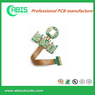
Larger photo of Multilayer Pcbs, Rigid-Flex High-Density Multilayer PCB Immersion Gold HASL-FL
Related products about Multilayer Pcbs, Rigid-Flex High-Density Multilayer PCB Immersion Gold HASL-FL
-
 Waste Tyre Plastic Recycling Machinery Machine Tire Crusher Production Line Rubber Crumb Grinding Machine Equipment Tire Shredder
-
 Stretch Plastic Blowing Pet Bottle Making Blow Molding Machine Bottles Stretch Automatic Pet Bottle Blowing Machine
-
 Waste Plastic Pet Bottle, Water Bottle Flake, PP/HDPE/LDPE PE Film Jumbo Woven Bags Plastic Crusher Machine, Plastic Crushing Washing Recycling Machine
-
 Type 2 Wall-Mounted Electric Car Charging Station 7kw /11 Kwelectric Vehicle Charging Station Home Wallbox AC EV Charger Single Phase or 3three Phase
-
 G-View G12W Wholesale Auto Car LED Headlight Bulb High Power H13 H11 9005 H7 H4 Car LED Headlights LED Car Lights
-
 New Design Porcelain Round Plates Dinner Set for Wedding and Banquet
-
 China 2023 New Design Super Soft 100% Polyester Microfiber Knitted Oversized Decoration Hoodie Blanket
-
 Handmade Art Creative Materials Thickened White Paper Cup DIY Disposable Handmade Colored Paper Cup


